


SI5340A-D07099-GM Specifications
Manufacturer: Skyworks Solutions, Inc.
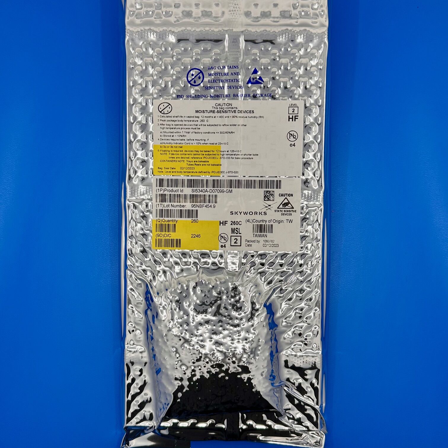
Part Number: SI5340A-D07099-GM
Product Type: Programmable Clock Generator
Number of Outputs: 4
Input Frequency Range: 10 MHz to 750 MHz (differential), 10 MHz to 250 MHz (LVCMOS), 25 MHz to 54 MHz (external crystal)
Output Frequency Range: 100 Hz to 1028 MHz (differential), 100 Hz to 250 MHz (LVCMOS)
Output Signal Formats: LVDS, LVPECL, LVCMOS, CML, HCSL
RMS Phase Jitter: 90 fs (typical)
Core Supply Voltage (VDD): 1.8V ±5%
Analog Supply Voltage (VDDA): 3.3V ±5%
Output Supply Voltage (VDDO): 1.8V, 2.5V, or 3.3V
Package / Case: 44-QFN (7mm x 7mm)
Mounting Type: Surface Mount
Operating Temperature Range: -40°C to +85°C
RoHS Status: RoHS Compliant
Key Features
The SI5340A-D07099-GM is a highly flexible, low-jitter clock generator capable of synthesizing any combination of output frequencies from any input frequency. Its ultra-low jitter performance of 90 fs RMS makes it suitable for high-performance applications. The device supports a wide input frequency range, accommodating external crystals from 25 MHz to 54 MHz. Differential clocks from 10 MHz to 750 MHz, and LVCMOS clocks from 10 MHz to 250 MHz. Supports various signal formats such as LVDS, LVPECL, LVCMOS, CML, and HCSL, with programmable signal amplitude. In Addition, this device operates with a core supply voltage of 1.8V and an analog supply voltage of 3.3V, while output drivers can be powered by 1.8V, 2.5V, or 3.3V supplies. Its compact 44-QFN package facilitates integration into space-constrained designs.
Applications
Clock tree generation replacing XOs, buffers, and signal format translators
Any-frequency clock translation
Clocking for FPGAs, processors, and memory
Ethernet switches and routers
OTN framers, mappers, and processors
Test equipment and instrumentation
Broadcast video systems
Product Overview
The SI5340A-D07099-GM clock generator offers a versatile solution for complex timing requirements in modern electronic systems. Its ability to generate any combination of output frequencies from various input sources simplifies clock tree design, reducing the need for multiple discrete components. The device’s ultra-low jitter performance ensures high signal integrity, which is crucial for applications like high-speed networking and data communications. The programmable output formats and amplitudes provide designers with the flexibility to tailor the clock signals to specific system requirements. Additionally, the device’s compact QFN package and surface-mount design facilitate easy integration into densely populated PCBs.
Contact Us
For additional information regarding our products, feel free to get in touch with us. You can call us at 770-870-1760 or email us at info@Cyndtek.com. We look forward to assisting you and ensuring your satisfaction with all of our Cyndtek products.
For additional available stock, browse our full inventory.


Reviews
There are no reviews yet.